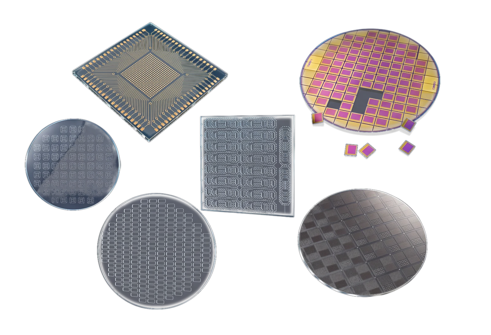
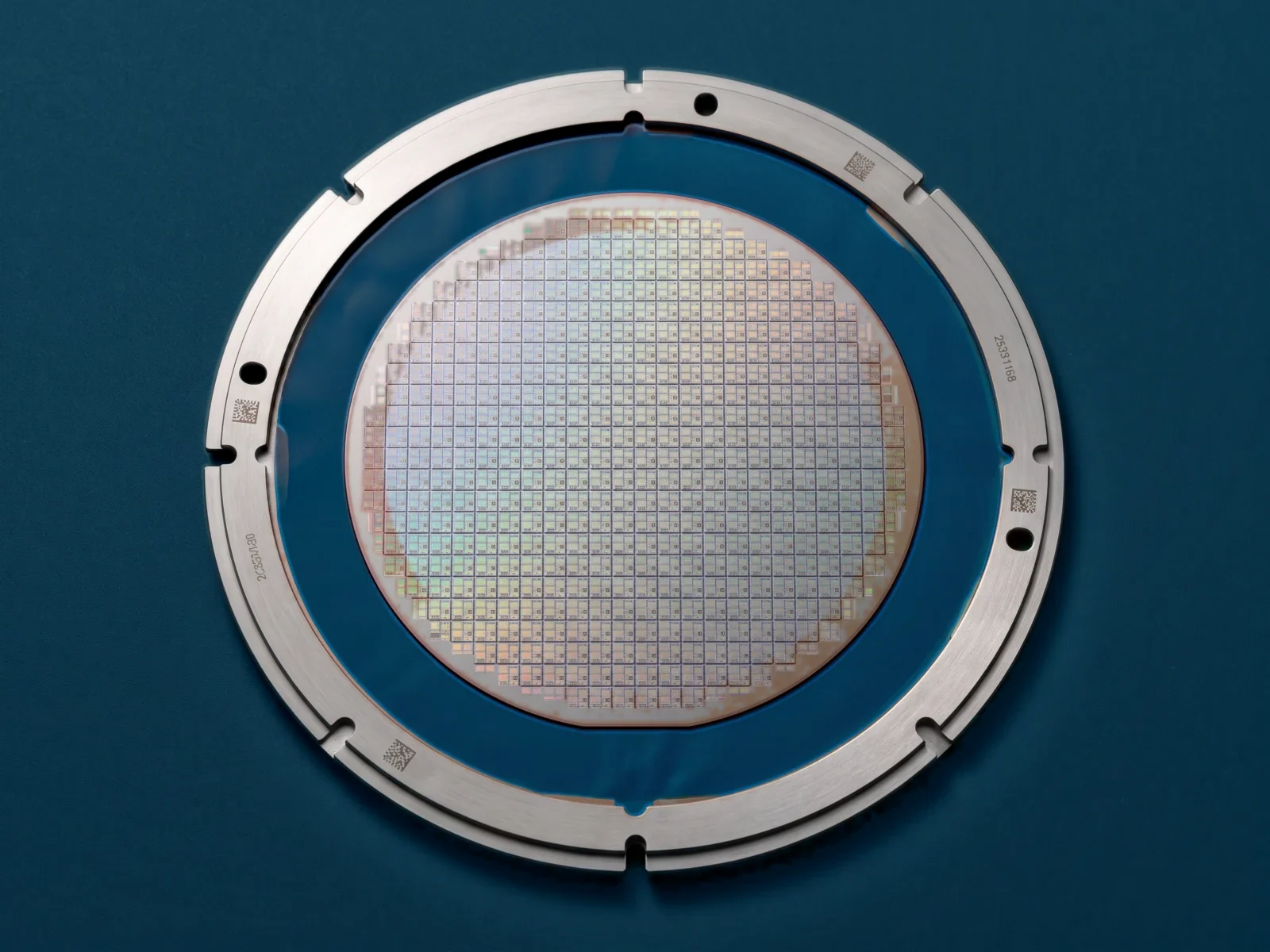
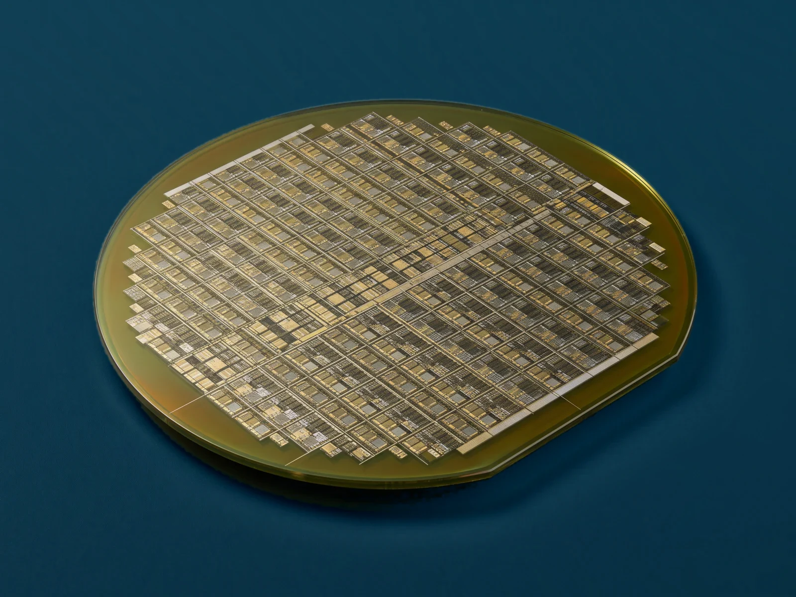
Dicing and grooving of thin wafers, SiC processing, and drilling and cutting of glass core substrates, interposers and MEMS wafers. Femtosecond pulses remove material before heat spreads, so dies keep more of their strength and glass edges show minimal cracking.
Where femtosecond processing works across the wafer and the package, from the first dicing cut to the finished substrate.
Wafer dicing and grooving
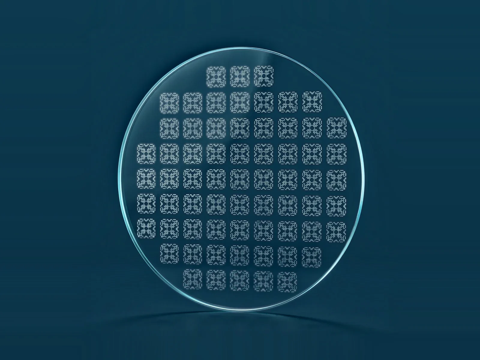
Mechanical blade dicing chips the die edge and limits how thin a wafer can get before it cracks under the blade. Femtosecond pulses cut or groove the wafer with a narrow kerf and little debris. On wafers with low-k dielectric stacks, a laser groove first removes the brittle top layers along the street, so the cut that follows does not peel or crack them. Grooving followed by dicing is now a common sequence for advanced logic and memory wafers.
Silicon carbide and other wide-bandgap materials go into electric vehicles, fast chargers and RF devices. They are harder and more brittle than silicon, so a diamond saw wears fast and leaves chipping along the cut. Femtosecond pulses dice the wafer and trim its edge with far less of that chipping, and the same laser scribes GaN, sapphire and other hard substrates.
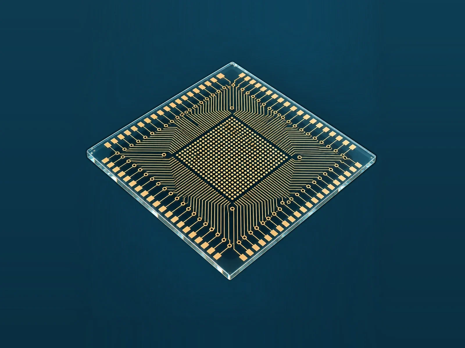
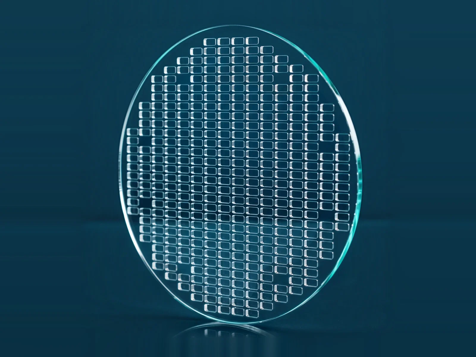
The largest AI and high-performance packages are outgrowing organic cores, which warp under heat and limit how fine the wiring can be. A glass core stays flat, expands with temperature much like silicon and takes finer lines. The laser writes the vias through the core and cuts the panel into substrates with minimal chipping along the edge.
Thinner wafers, smaller dies. Less room for damage.
Wafers keep getting thinner, dies smaller and packages larger. Every step leaves less margin for chipping, cracks and heat damage.
Blades chip, heat damages
As wafers get thinner and dies smaller, blade dicing causes chipping and cracks. Longer-pulse lasers leave heat damage and debris that lower die strength and yield.
What the process needs
Narrow kerf with minimal chipping
Minimal heat damage to nearby structures
Clean processing with little debris
Throughput that fits fab cycle times
Remove material with minimal heat
Femtosecond pulses ablate thin layers of silicon, low-k films and other materials before heat spreads, giving narrow, clean cuts and grooves on fragile wafers.
Through-glass vias
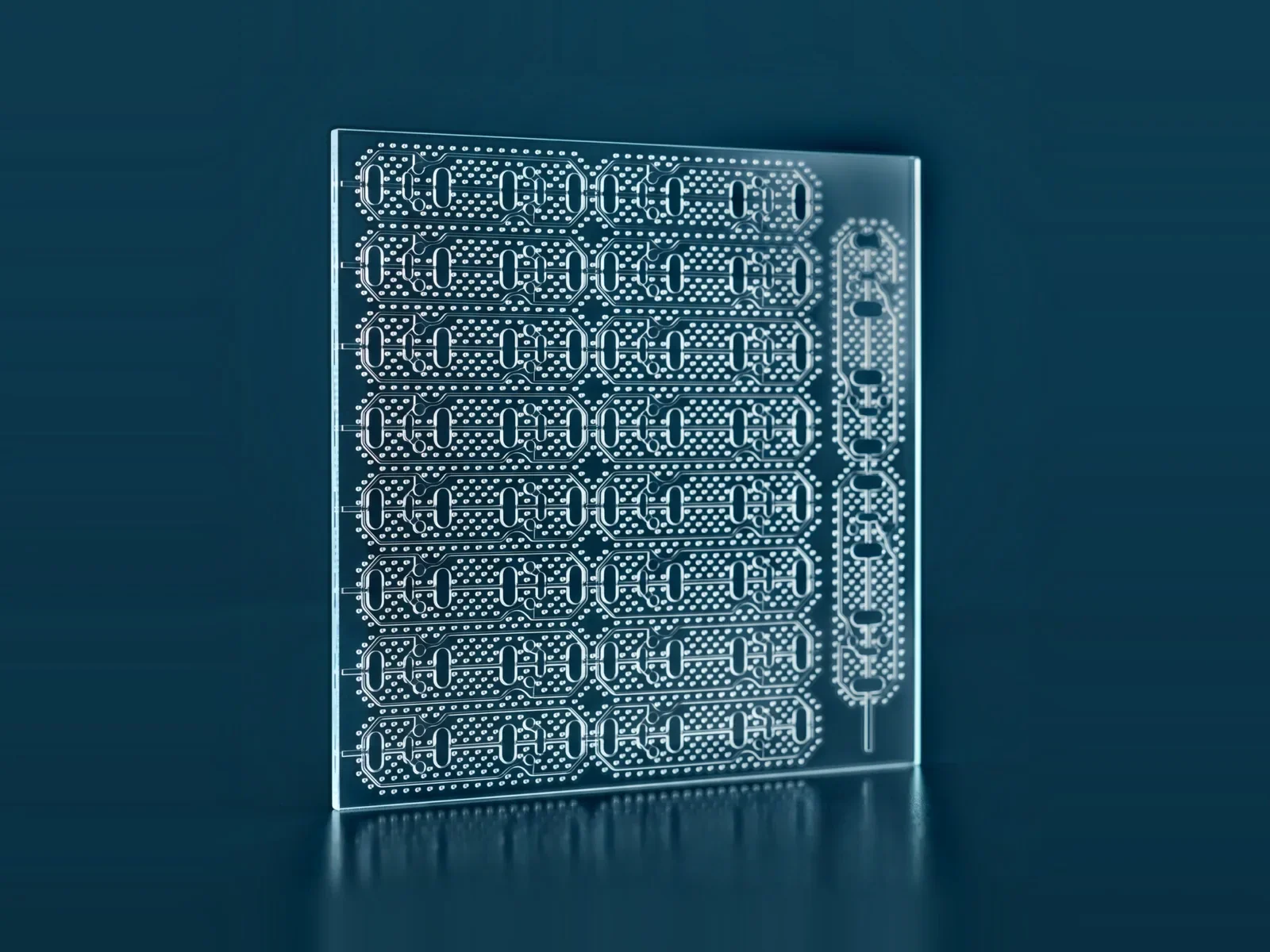
Through-glass vias give advanced packages a dense, low-loss vertical interconnect at panel scale. Each via is written through the glass by the laser in one shot, then opened by a selective wet etch, so a panel can hold millions of vias with smooth walls and minimal cracking.
In 2.5D packages an interposer carries chiplets side by side and routes signals between them through a redistribution layer (RDL) on its surface. The laser drills the interposer vias, opens dielectric layers ahead of plating and cuts the finished wafer or panel, with minimal heat load on the layers underneath.
Material
Glass and silicon interposers, dielectric layers
Process
Via drilling, selective ablation ahead of RDL plating, singulation
Many MEMS sensors and RF filters are sealed under a glass cap wafer. The cap needs a cavity above each device and through-holes for the electrical contacts, and both have to be free of cracks to keep the seal tight. Laser modification and etching form the cavities and holes in one process, and the laser then cuts the bonded stack into single dies.
A femtosecond pulse removes material before heat can spread into the wafer. The kerf stays narrow, the die edge has little chipping and a minimal heat-affected zone, and thin dies keep more of their bending strength than after blade dicing.
What is the difference between grooving and dicing?
Grooving removes only the top layers along the dicing street, such as low-k dielectric and metal test structures, so they do not peel or crack. Dicing then cuts through the full wafer, either with a blade or with the laser. Many advanced wafers are grooved first and diced second.
Femtosecond or nanosecond laser for low-k grooving?
Nanosecond lasers groove fast but melt the edges of the groove and leave recast and debris that can lift low-k films. Femtosecond pulses remove the layers with far less heat, which gives cleaner groove walls and a smaller risk of delamination.
Can a femtosecond laser dice SiC wafers?
Yes. Silicon carbide is hard and brittle, so diamond saws wear quickly and leave chipping. Femtosecond pulses ablate SiC without mechanical contact and are also used for scribing, edge trimming and marking on SiC, GaN and sapphire.
How thin can a wafer be for laser dicing?
Laser processing works on wafers down to a few tens of micrometres, where blade dicing struggles. The limit is usually handling and the tape frame, not the laser.
What are glass core substrates?
Glass core substrates replace the organic core of large chip packages with a glass panel. Glass stays flat, matches the thermal expansion of silicon closely and carries finer wiring. Signals pass through the core in through-glass vias, which are written by the laser and opened by wet etching.
Which LITILIT laser fits semiconductor processing?
Indylit 20 covers most wafer and glass work: over 200 µJ per pulse for glass and SiC, pulse duration tunable from 400 fs to 4 ps and an optional 515 nm module. Indylit 10 suits lighter structuring and marking jobs.
How does buying a laser work?
Tell us your material, process and volume. An application engineer reviews your request and suggests a laser and configuration. You then receive a quotation with pricing, lead time, payment and support terms.
Tell us your material, process and volume. Our application engineers suggest a laser and configuration, and we send a quotation with pricing, lead time and support terms.