Through-glass vias (TGV)

Through-glass vias for glass core substrates and interposers. How laser modification and selective wet etching work, what the process can reach, and which femtosecond laser fits.

Millions of vias per panel. Each one clean and consistent.

Glass is starting to replace organic cores in advanced packages because it stays flat, stable and smooth at the line widths AI and HPC chips need. The hard part is the vias.

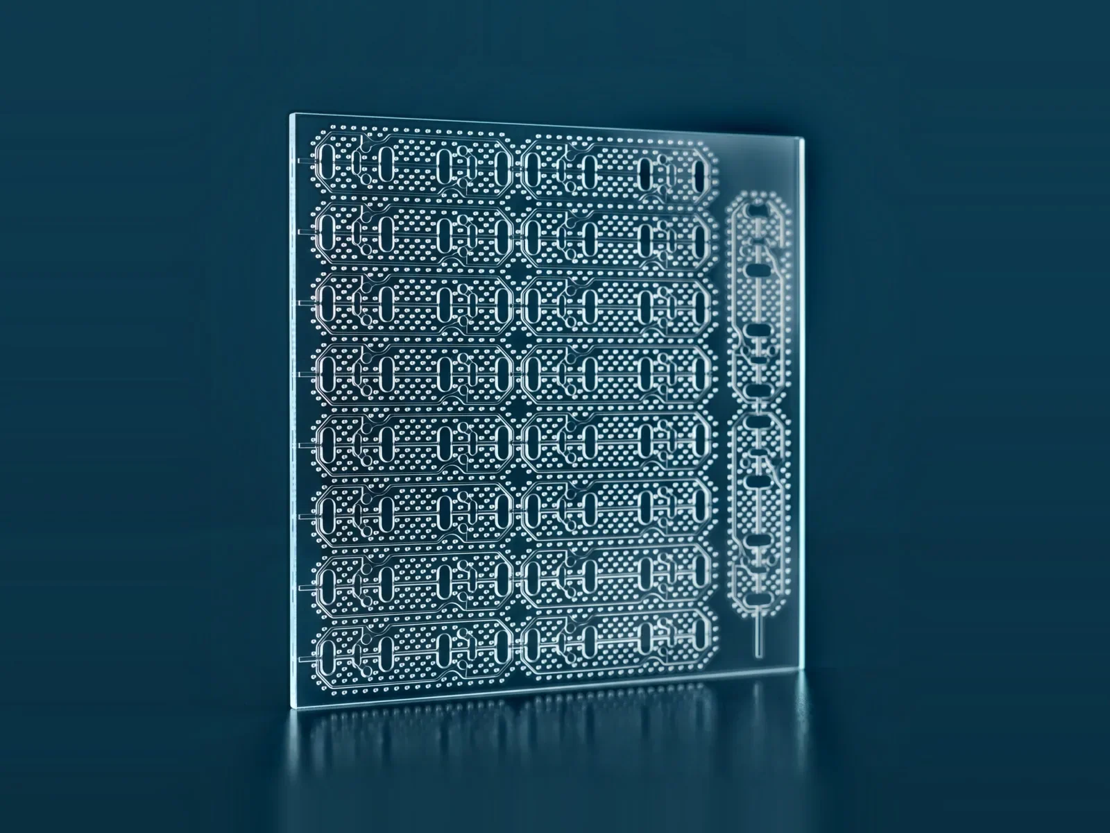
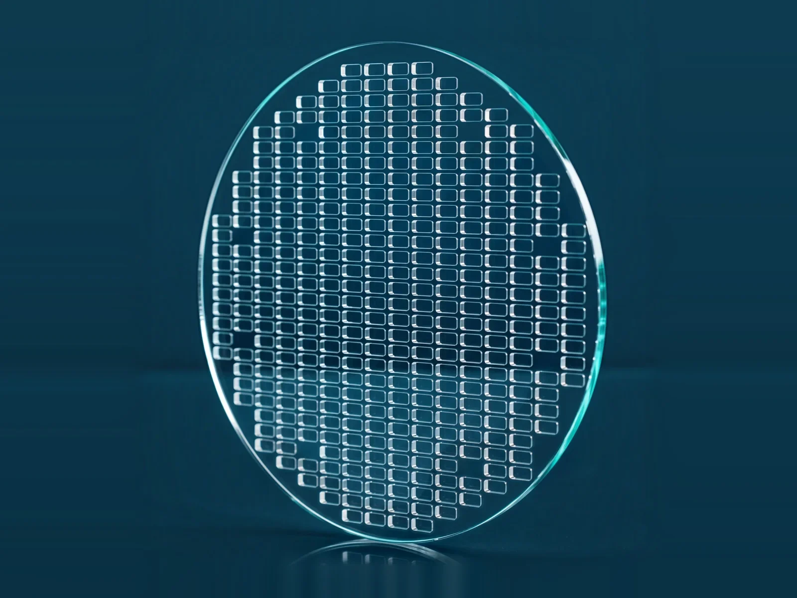
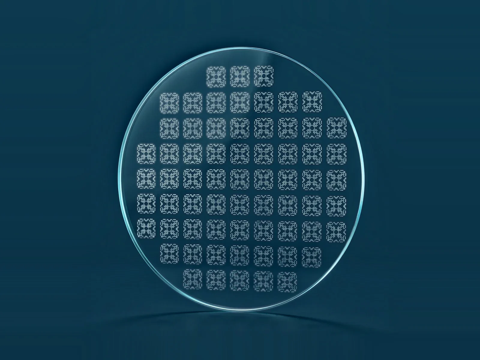
Glass interposer wafer with repeated through-glass via fields
  1. Drilling cracks the glass

    Mechanical drills, CO₂ and nanosecond lasers remove glass with force or heat. They leave microcracks, heat-affected zones and tapered walls around each via, and those defects grow into failures in thermal cycling and reliability testing.

  2. What the process needs

    • Via walls with minimal cracking and heat-affected zone
    • Straight, low-taper vias at high aspect ratio
    • Micron-level position accuracy across the whole panel
    • Thousands of vias per second for panel-level throughput
  3. Modify first, then etch

    A femtosecond pulse is absorbed only where it is focused inside the glass. It changes the glass along the via path without removing material and with minimal cracking. A wet etch then dissolves the modified glass far faster than the untouched bulk and opens a clean, straight via.

How TGV drilling works.

TGV drilling with a femtosecond laser is a two-step method, also known as selective laser etching (SLE). The laser writes, the etch bath opens, and each step can be tuned on its own.

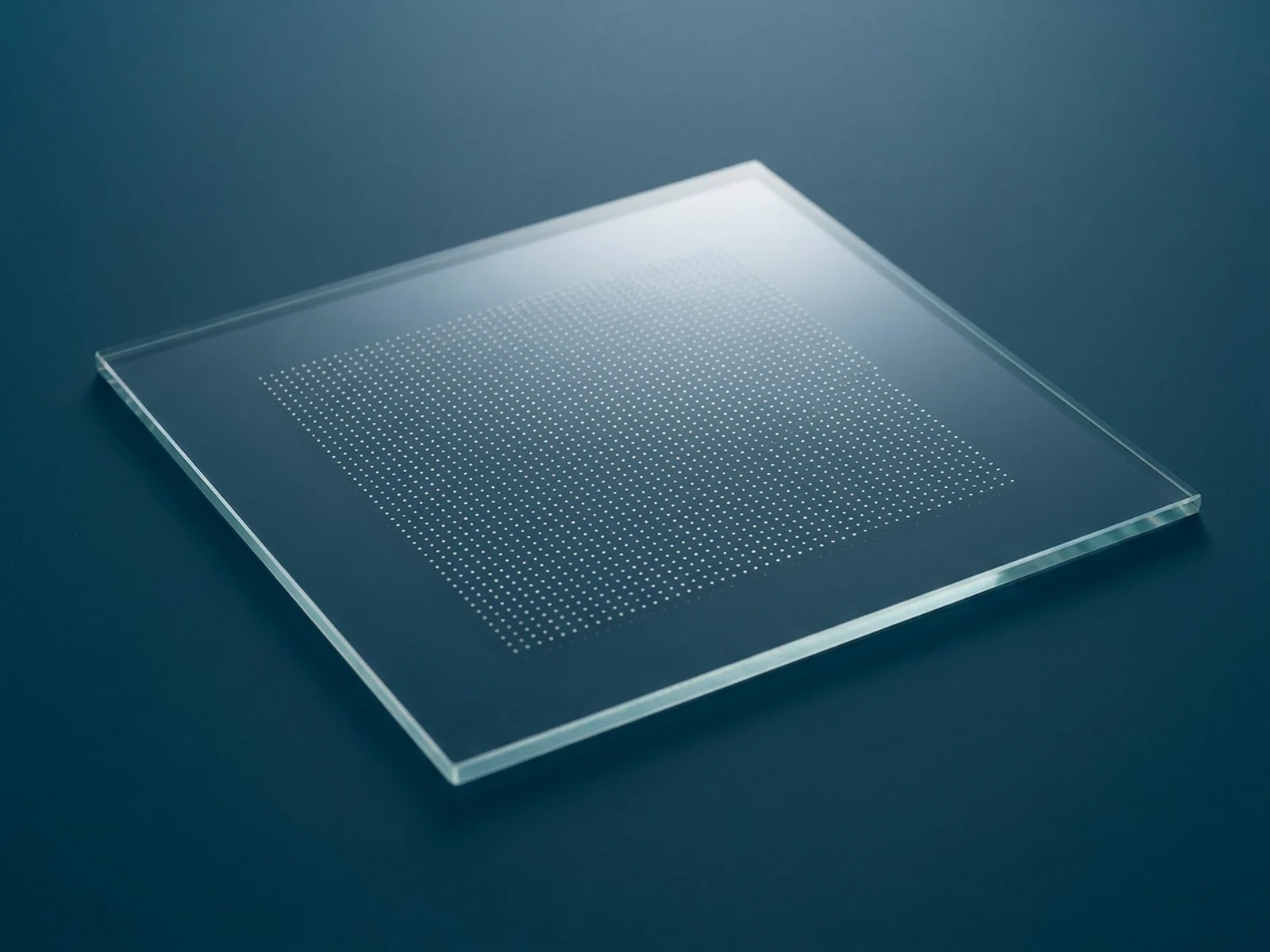
Glass panel with a regular grid of laser-written vias

Laser modification

Beam-shaping optics stretch the focus into a long, thin line that reaches through the full thickness of the glass. One pulse or one short burst per via changes the glass along that line. Nothing is removed yet, so there is no debris or recast, and with the right settings cracking is kept to a minimum. Pulse energy is matched to the glass thickness, and splitting each shot into a burst evens out the modification through the depth. Writing speed is set by the motion system and reaches thousands of vias per second.

Pulses per via
One pulse or one short burst
Focus
Elongated line focus through the full thickness
Pulse duration
Tuned per glass, 400 fs to 4 ps
Suggested laser
Indylit 20
Glass panel with etched vias, channels and openings

Selective wet etching

The whole panel goes into an etch bath. The laser-modified glass dissolves many times faster than the untouched glass around it, so the via opens along the written line while the surface barely changes. The etchant, its temperature and the etch time set the final diameter and the taper. Alkaline etchants give higher selectivity than hydrofluoric acid and are easier to handle in production.

Etchants
Hydrofluoric acid, KOH or NaOH
What it sets
Final via diameter and taper
Thin glass panels of different thickness used for through-glass vias

Glass types and thickness

The method works on the glasses used for packaging and display: borosilicate, alkali-free aluminosilicate, fused silica and soda-lime. Each glass reacts to the laser and to the etchant differently, so the process window is set per glass type and thickness.

Glass
Borosilicate, alkali-free, fused silica, soda-lime
Thickness
From 50 µm thin glass to 1 mm cores
Format
Wafers and large rectangular panels

Where through-glass vias are used.

The same laser-written via ends up in very different products. What they share: glass that stays flat and stable, and clean, consistent vias.

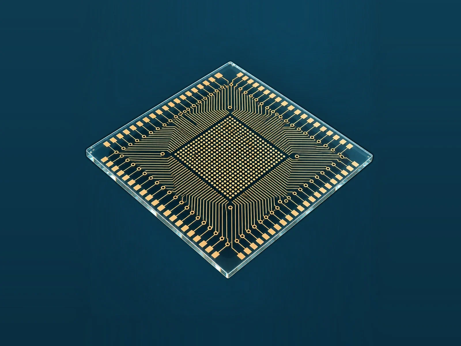
Glass core substrate with copper-filled vias and fan-out wiring

Glass core substrates

The largest chiplet packages for AI and high-performance computing are outgrowing organic cores, which warp under heat and limit how fine the wiring can be. A glass core stays flat, expands with temperature much like silicon and takes finer lines on its surface. Every signal and power path through the core runs in a through-glass via, so one panel holds hundreds of thousands of them or more.

Why glass
Flatness, dimensional stability, fine-line wiring
Via role
Signal and power through the core
Glass interposer wafer with repeated through-glass via fields

Glass interposers

In 2.5D packages an interposer sits between the chips and the substrate and carries thousands of short connections between them. Glass interposers do this at lower cost than silicon, come in large panel formats and add very little electrical loss, which matters more as data rates between chiplets climb.

Alternative to
Silicon interposers
Via role
Vertical links between chips and substrate
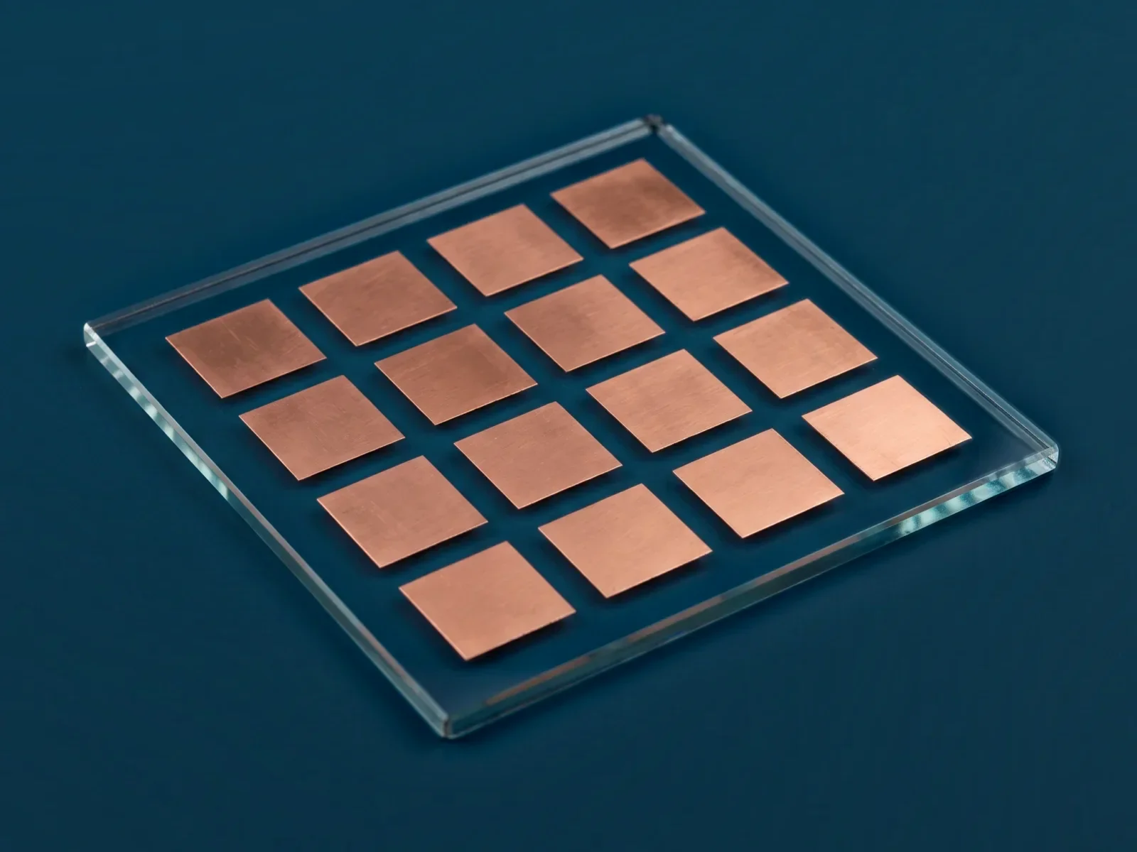
Glass substrate with a 4 by 4 copper patch antenna array for 5G modules

RF and antenna-in-package modules

At millimetre-wave frequencies every bit of dielectric loss counts. Glass has low loss and a stable dielectric constant, so 5G and radar modules use it to carry antennas, filters and integrated passive devices. Through-glass vias connect the antenna layer on top to the RF chip below and form shielding walls around sensitive lines.

Why glass
Low dielectric loss at high frequency
Via role
Antenna feeds, ground and shielding
Glass cap wafer with etched cavities for MEMS packaging

MEMS and sensor packaging

Motion sensors, pressure sensors and microphones are sealed under a cap wafer that protects the moving structure. A glass cap is transparent for alignment and inspection and bonds well to silicon. Through-glass vias carry the electrical contacts out of the sealed cavity, so the device is packaged at wafer level without wire bonds.

Format
Glass cap wafers bonded to silicon
Via role
Contacts out of a sealed cavity
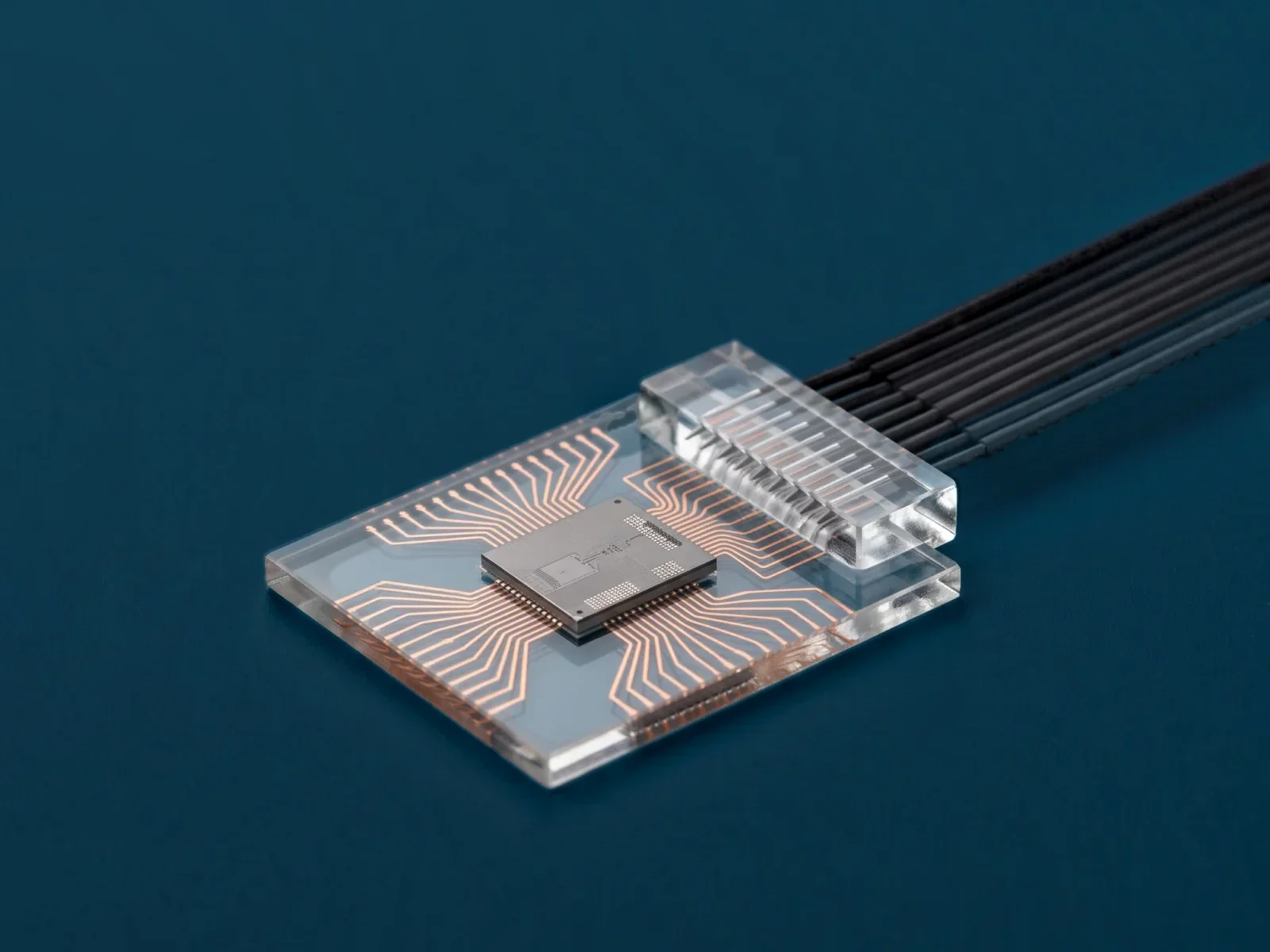
Glass interposer with a photonics chip and an attached fiber array

Co-packaged optics

Data-centre switches are moving optical links right next to the processor. Glass interposers combine both worlds: the vias carry power and high-speed electrical signals, while waveguides and alignment features in the same glass guide light between the fibres and the photonic chip. Femtosecond lasers can write waveguides inside glass as well as vias.

Combines
Electrical vias and optical waveguides
Via role
Power and high-speed signals
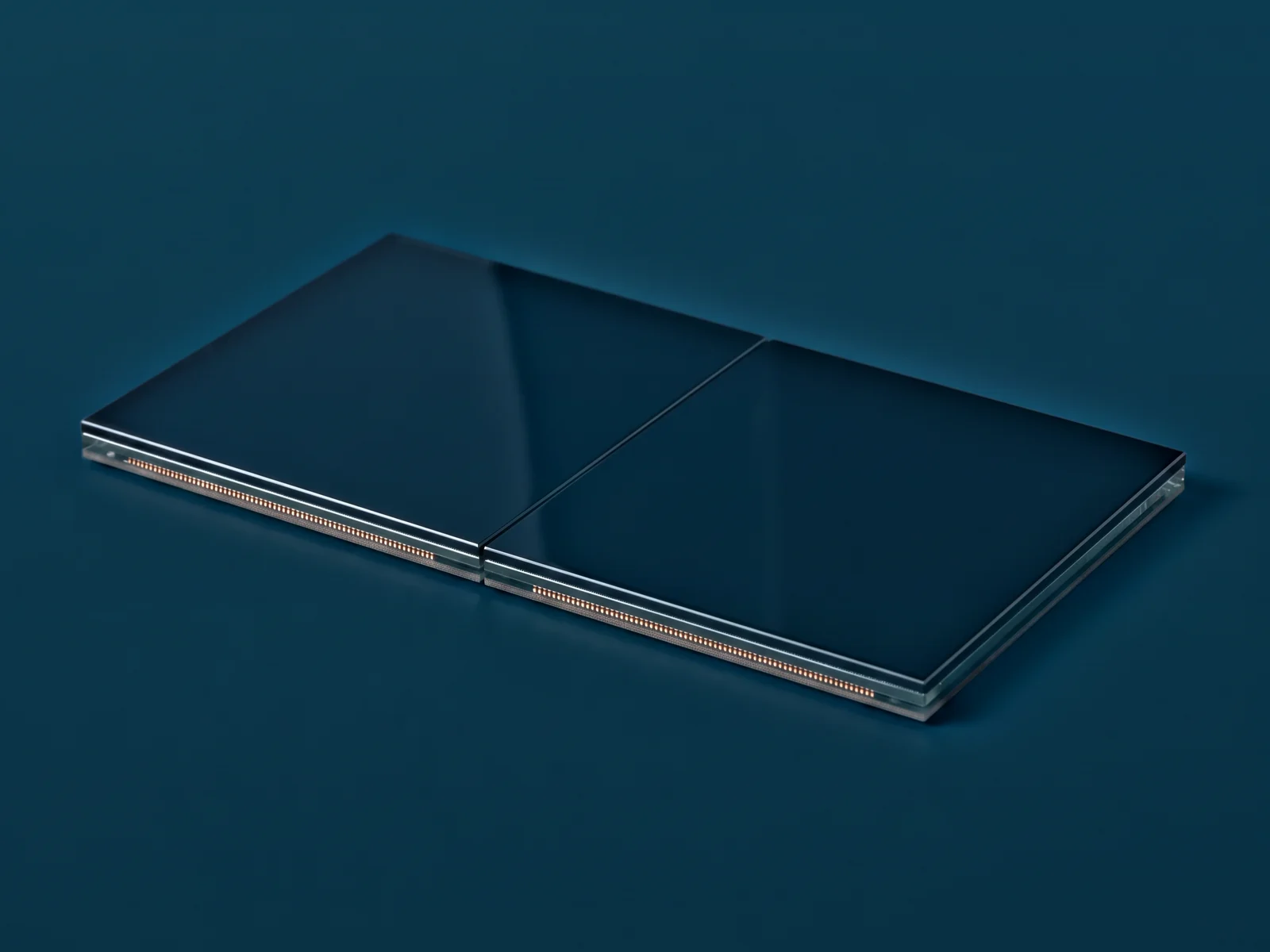
Two microLED display tiles on glass backplanes joined edge to edge

MicroLED display backplanes

Large microLED walls are built from tiles that have to join without a visible seam. Routing the driver lines through the glass backplane instead of around its edge removes the bezel, so tiles can sit edge to edge. Through-glass vias make that back-side connection possible on thin display glass.

Goal
Seamless, bezel-free tiling
Via role
Driver lines to the back side
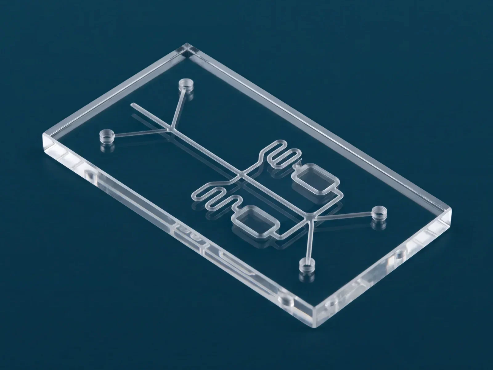
Glass microfluidic chip with etched channels, chambers and through-hole ports

Microfluidics and lab-on-chip

Lab-on-chip devices for diagnostics and cell research are made of glass because it is clear, inert and easy to clean. The same modify-and-etch method that opens vias also cuts inlet and outlet ports and forms channels inside the glass, so a whole chip is structured in one process, with minimal cracking that could trap liquid.

Why glass
Optically clear, chemically inert
Holes for
Inlet and outlet ports, channels

Glass via drilling methods compared.

There are several ways to put a hole through glass. Only some of them leave a via that survives reliability testing.

Mechanical drilling
Chipping and microcracks; limited to larger holes
CO₂ laser drilling
Heat-affected zone, cracks and tapered walls
Nanosecond and picosecond ablation
Debris, recast and taper; slow in thick glass
Photo-structurable glass
Needs a special glass, UV exposure and heat treatment
Femtosecond modification and wet etching
Straight vias in standard glass with minimal cracking; one shot per via

Typical TGV process window.

Ranges reported for laser modification and wet etching, plus the layout rules that keep a design easy to produce. Your glass, thickness and via design will move them, so every number has to be confirmed on your own glass.

Glass types
Borosilicate, alkali-free, fused silica, soda-lime
Glass thickness
50 µm – 1 mm
Via diameter
From about 5 µm, larger in thicker glass
Aspect ratio
Around 1:10 routine, up to 1:50
Taper
Below 1° with alkaline etching
Via pitch
At least about twice the via diameter
Edge keep-out
Vias kept clear of panel edges and dicing lanes
Feature shapes
Round vias, slots, cavities, alignment marks
Recommended laser
Indylit 20

TGV quality: what to measure.

A via is only as good as the plating and the reliability test it passes. These are the checks that tell you it will.

Diameter and waist
Top, bottom and narrowest diameter, and their spread across the panel
Taper and shape
The same profile on every via, so seed layer and plating stay tuned
Wall roughness
Smooth walls for a void-free copper fill
Position accuracy
Every via on its pad, with no drift over a long run
Edges and strength
No chipping at entry or exit; bending strength kept
Inspection
Automated optical check of every via after etching

Questions about TGV.

What is a through-glass via?

A through-glass via (TGV) is a vertical electrical connection through a glass substrate. A hole is made through the glass and then filled or lined with copper, so signals and power can pass from one side to the other. TGVs are used in glass core substrates, glass interposers, RF modules and MEMS packages.

Why use glass instead of silicon or organic substrates?

Glass stays flat at large sizes, its thermal expansion can be matched closely to silicon, it has low electrical loss at high frequencies and it is made in large panels at a lower cost than silicon wafers. Organic cores warp under heat, and silicon interposers are limited by wafer size and cost.

Why a femtosecond laser for TGV?

A femtosecond pulse deposits its energy before heat has time to spread. Inside transparent glass it is absorbed only in the focus, so it changes the glass along the via path with minimal melting or cracking. Longer pulses heat the surrounding glass, which leads to stress, microcracks and taper.

How small and how deep can the vias be?

Published results with laser modification and wet etching reach via diameters down to about 5 µm and aspect ratios up to about 1:50, in glass from 50 µm to 1 mm thick. The final diameter and taper are set mainly by the etch step, so they are tuned to each design.

How are the vias metallised?

After etching, the vias are cleaned, coated with a thin seed layer and filled or lined with copper by electroplating. Metallisation is where via quality shows: straight, smooth walls let the seed layer cover the wall evenly and the copper fill without voids.

How does buying a laser work?

Tell us your material, process and volume. An application engineer reviews your request and suggests a laser and configuration. You then receive a quotation with pricing, lead time, payment and support terms.

How many vias per second are possible?

The laser step is rarely the limit. Each via needs only a short burst of pulses, so the speed is set mostly by how fast the beam or the panel moves between positions. With on-the-fly triggering, a single head modifies thousands of vias per second, and more heads on one machine multiply the throughput.

Femtosecond or picosecond pulses for TGV?

Both are used. Shorter pulses give the most precise, low-stress modification; slightly longer pulses can modify thicker glass in one pass and speed up the etch. Indylit 20 lets you tune the pulse duration from 400 fs to 4 ps, so the best setting can be found on your glass rather than fixed by the laser.

Which glass works best?

Borosilicate and alkali-free display-type glasses are the most common choice for glass core substrates and interposers. Fused silica is used where low loss at high frequencies or optical clarity matters most. The right glass depends on thermal expansion, dielectric properties, panel size and cost, and each type needs its own laser and etch settings.

Does the laser leave stress in the glass?

The laser changes only a thin zone along the via path, and the etch removes most of that zone when it opens the via. With the right pulse energy and burst settings cracking around the via is kept to a minimum and the glass keeps its strength. Wrong settings show up quickly as microcracks or chipped edges, which is why the process window is set carefully for each glass.

Talk to us about your setup.

Tell us your material, process and volume. Our application engineers suggest a laser and configuration, and we send a quotation with pricing, lead time and support terms.