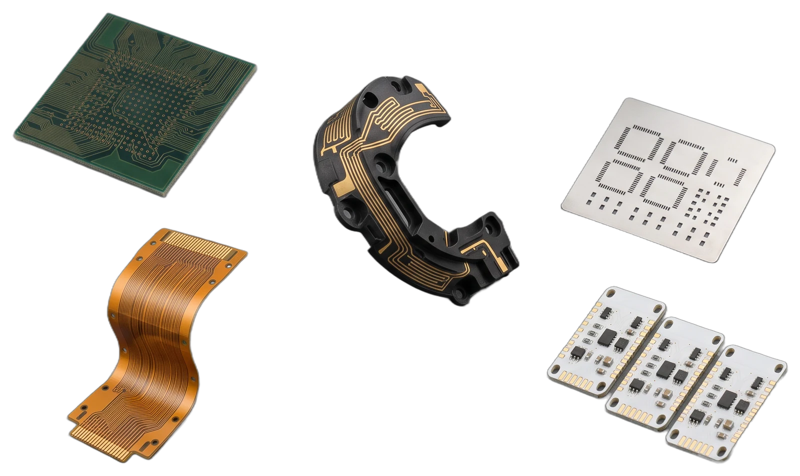
Cutting, drilling and structuring of flex circuits, PCBs, IC substrates, display films and ceramic circuits. Femtosecond pulses remove material before heat can spread, so thin layers stay clean and flat, with minimal carbonisation.
Where femtosecond processing works in electronics, from flex circuits and PCB depanelling to microvias, stencils, display films and ceramic circuits.
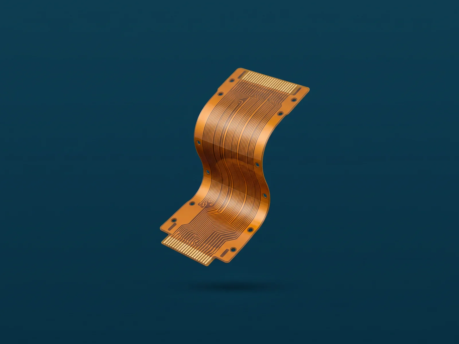
Flex PCB cutting
Polyimide flex circuits and coverlay are thin, soft and easy to char. The beam cuts outlines, slots and openings with little or no carbon on the edge and minimal delamination between layers, so the part needs little or no cleaning after cutting.
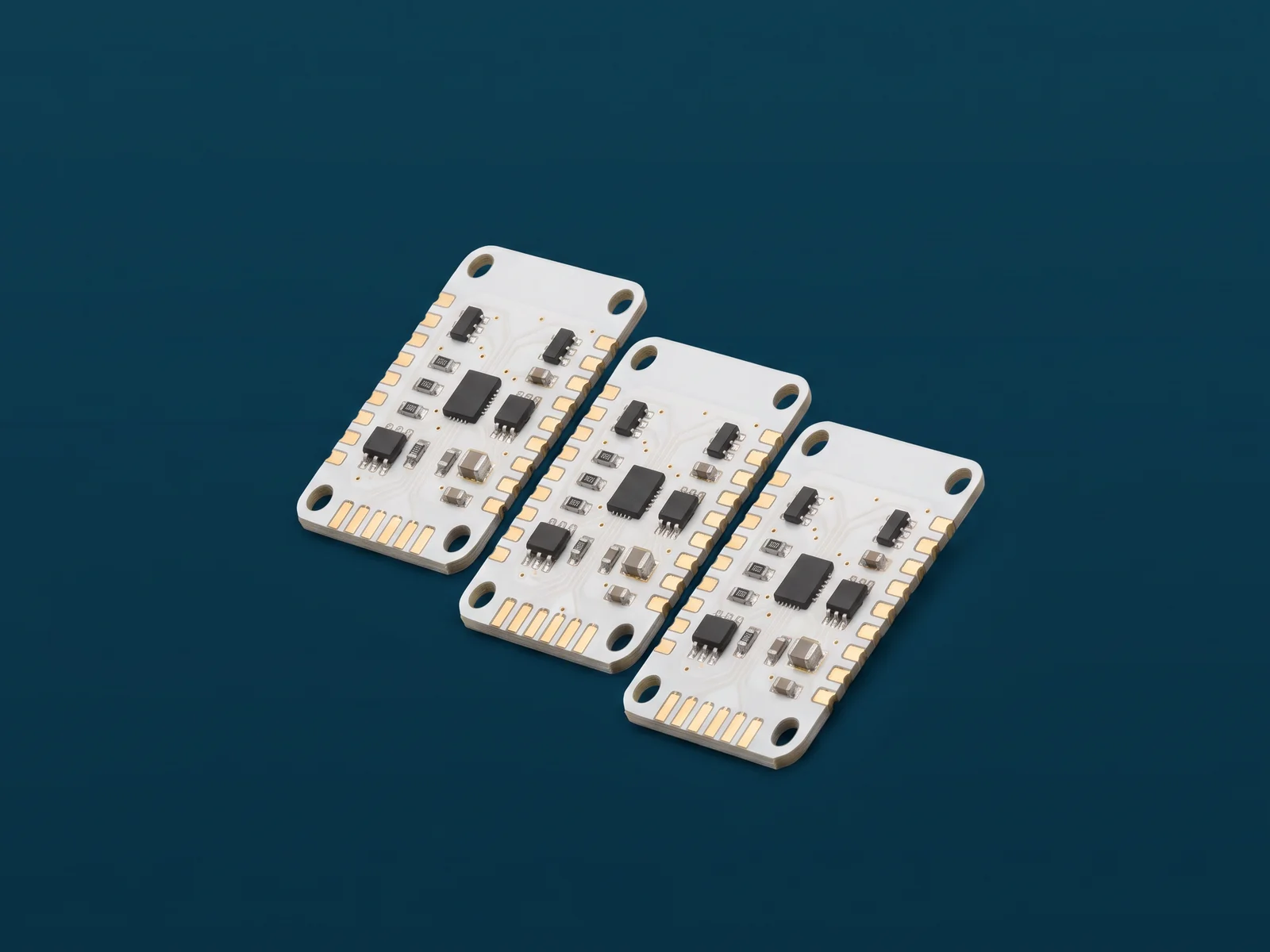
Populated boards are separated from the panel close to components and solder joints. A laser cut puts no mechanical load on the board, produces far less dust than routing and needs no tool change between board shapes.
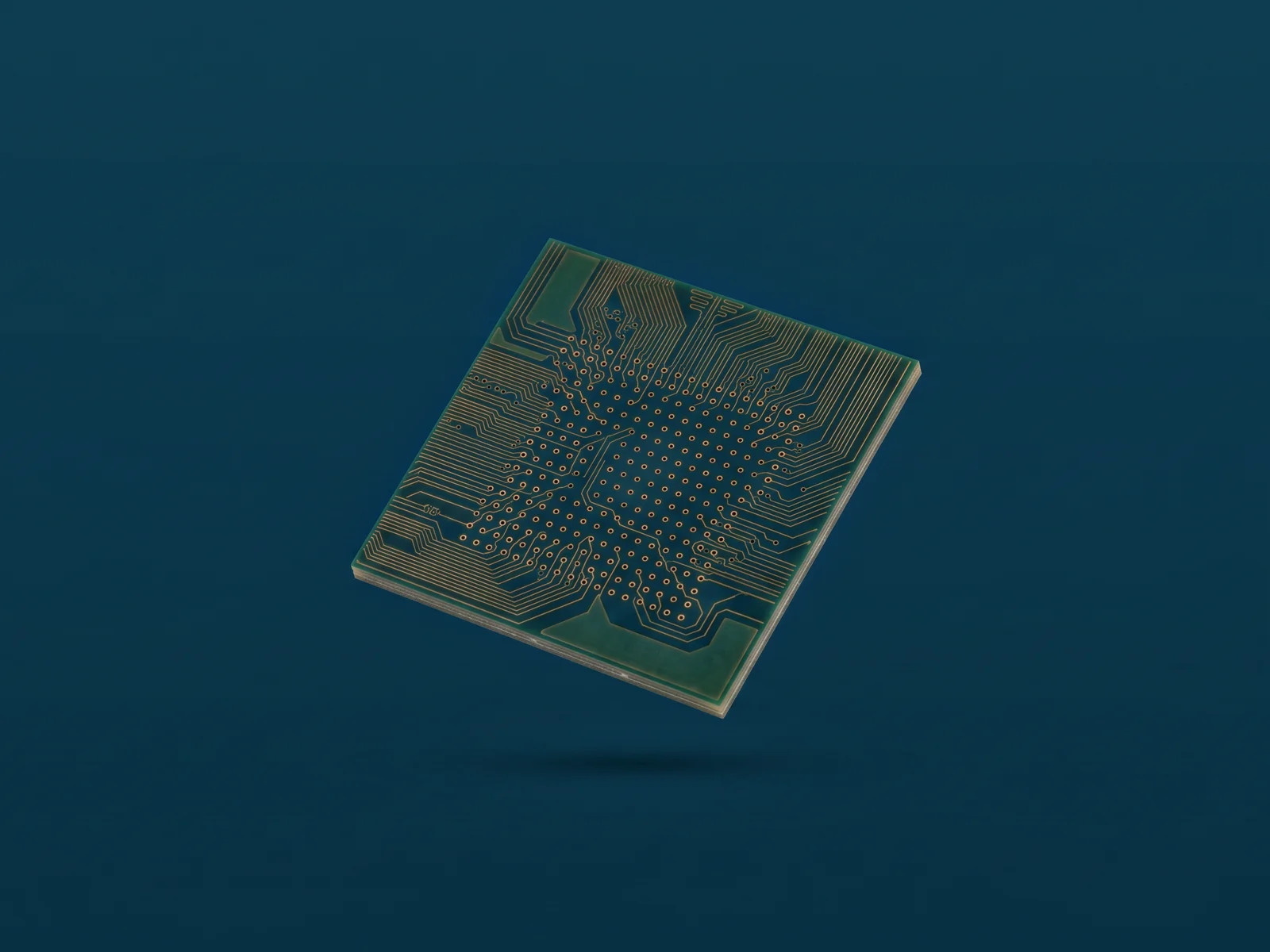
Blind and through microvias connect the fine layers of HDI boards and IC package substrates. Ultrashort pulses drill small, round vias through dielectric and copper with little resin residue at the bottom of the via.
Electronics keep shrinking: thinner polyimide, finer copper lines, smaller vias and components packed edge to edge. Mechanical tools and longer-pulse lasers leave burrs, dust, charred edges and stress that thin layers no longer tolerate.
Heat and force damage thin layers
Routers and punches stress thin boards and leave dust. CO₂ and nanosecond lasers char polyimide and epoxy, melt copper at the edge and leave a heat-affected zone that has to be cleaned or accepted.
What the process needs
Clean edges with little or no carbonisation on polyimide, FR-4 and films
No mechanical stress near components and solder joints
Tight positioning for fine pitch and small vias
One tool for different materials and layer stacks
Remove material, don't heat it
Femtosecond pulses ablate a thin layer at a time and are gone before heat can spread. Polymer, copper, glass and ceramic layers are cut with the same laser by changing the parameters, with a minimal heat-affected zone along the edge.
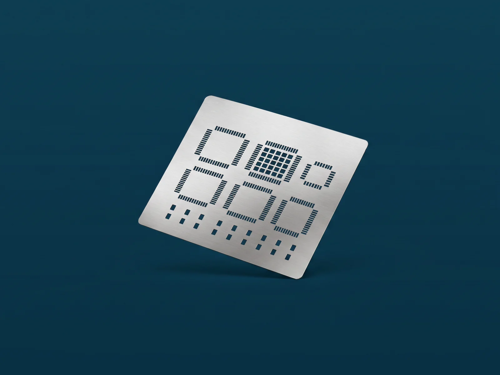
SMT stencils
Solder paste stencils need thousands of small apertures with smooth, straight walls so the paste releases cleanly. Femtosecond cutting leaves sharp aperture edges with minimal dross or burr, even in thin foils for fine-pitch parts.
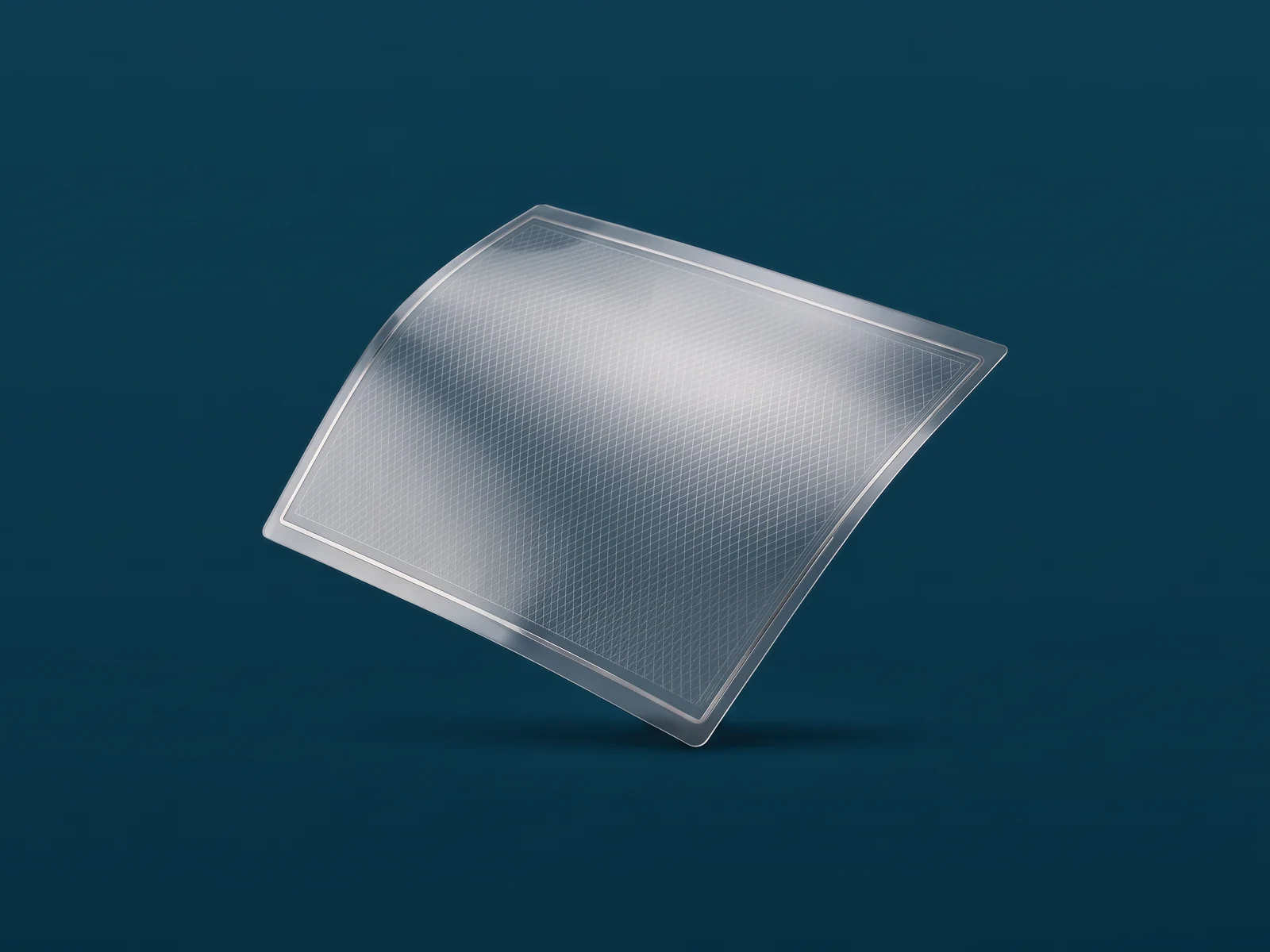
OLED panels, touch sensors and optical films are stacks of thin polymer, glass and conductive layers. The laser cuts shapes and openings, or removes a single coating, with minimal heat damage, the kind that shows up as dark edges or dead pixels.
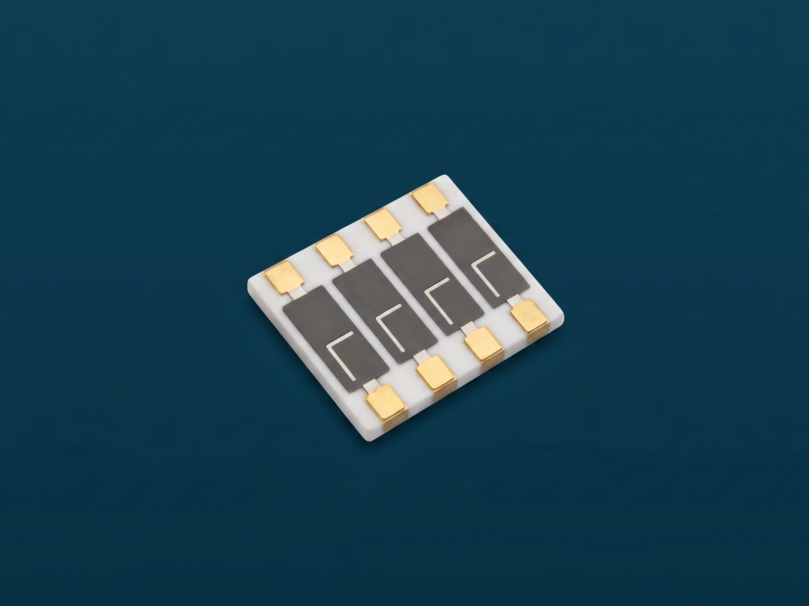
Alumina and aluminium nitride substrates carry power and sensor circuits. The laser scribes and cuts the ceramic, drills vias and trims thick-film resistors, with far fewer of the microcracks that heat and mechanical tools leave in brittle material.
Why use a femtosecond laser for PCB and flex cutting?
Femtosecond pulses remove material faster than heat can spread into it. Edges on polyimide and FR-4 show little or no carbonisation, copper hardly melts back and the risk of delamination in thin layers is minimal. That removes cleaning steps and lets cuts run closer to components.
Can the laser depanel populated boards?
Yes. Laser depanelling puts no mechanical load on the board and produces far less dust than routing, so it suits boards with components close to the cut line and parts that are sensitive to stress, such as ceramic capacitors.
Which materials can be processed?
Polyimide, coverlay and other polymer films, FR-4 and other laminates, copper, stainless steel stencil foils, thin glass and technical ceramics such as alumina and aluminium nitride.
How small can microvias be?
It depends on the dielectric, its thickness and the copper layers. Ultrashort pulses are used for vias of a few tens of micrometres in HDI boards and package substrates. Size and taper have to be confirmed on your own material.
Is a green wavelength needed?
Not always. The 1030 nm infrared output cuts most materials. The optional 515 nm green output of Indylit 20 is absorbed better by copper and many polymers, which helps on thin copper layers and fine features.
Which LITILIT laser fits electronics?
Indylit 20 for flex cutting, depanelling, microvias, stencils and ceramic circuits, where speed and pulse energy count. Indylit 10 for display films and smaller features where 10 W is enough.
How does buying a laser work?
Tell us your material, process and volume. An application engineer reviews your request and suggests a laser and configuration. You then receive a quotation with pricing, lead time, payment and support terms.
Tell us your material, process and volume. Our application engineers suggest a laser and configuration, and we send a quotation with pricing, lead time and support terms.