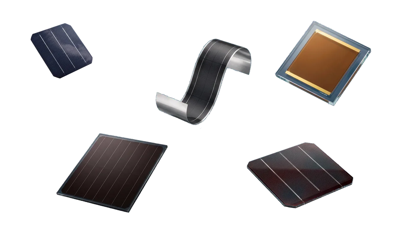
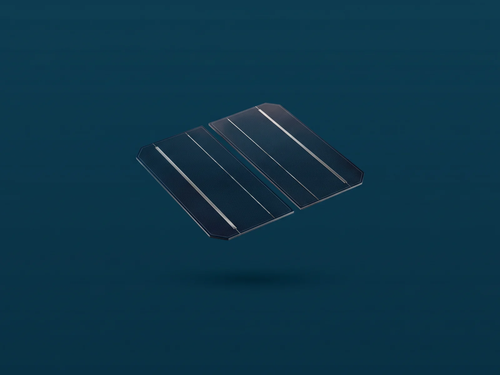
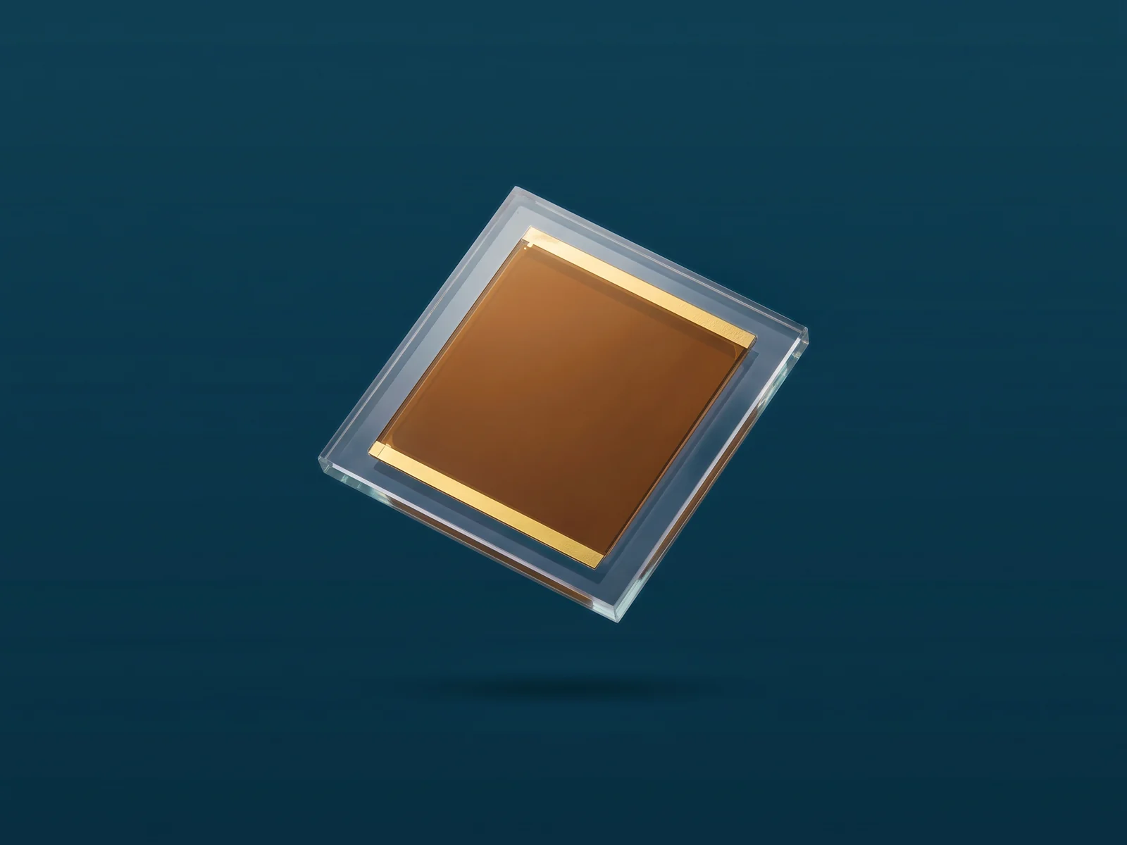
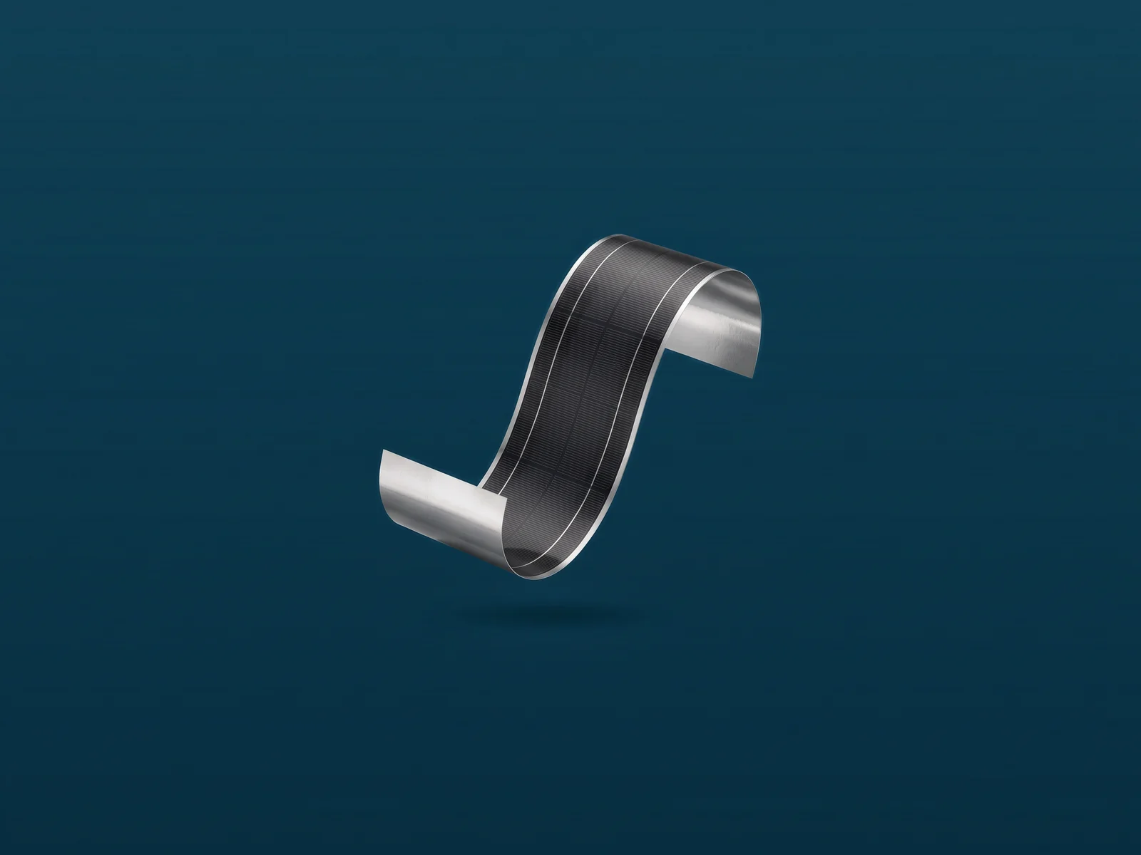
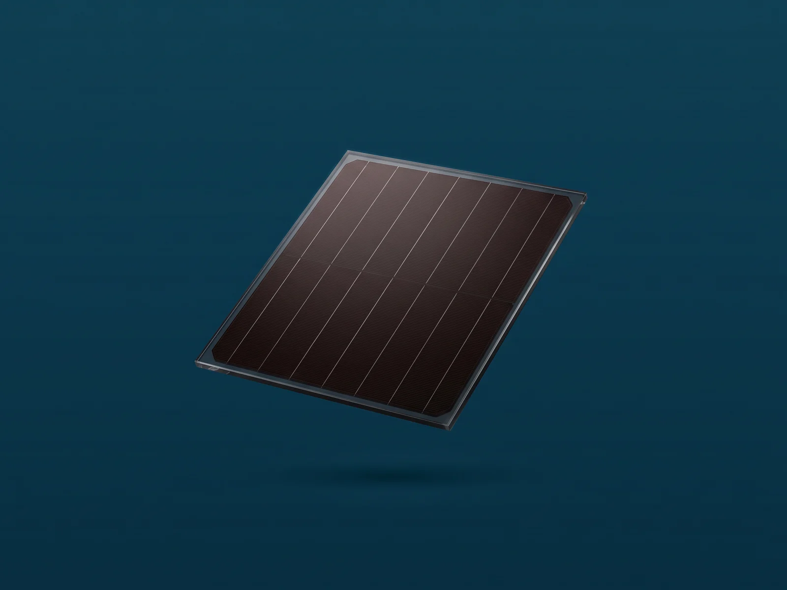
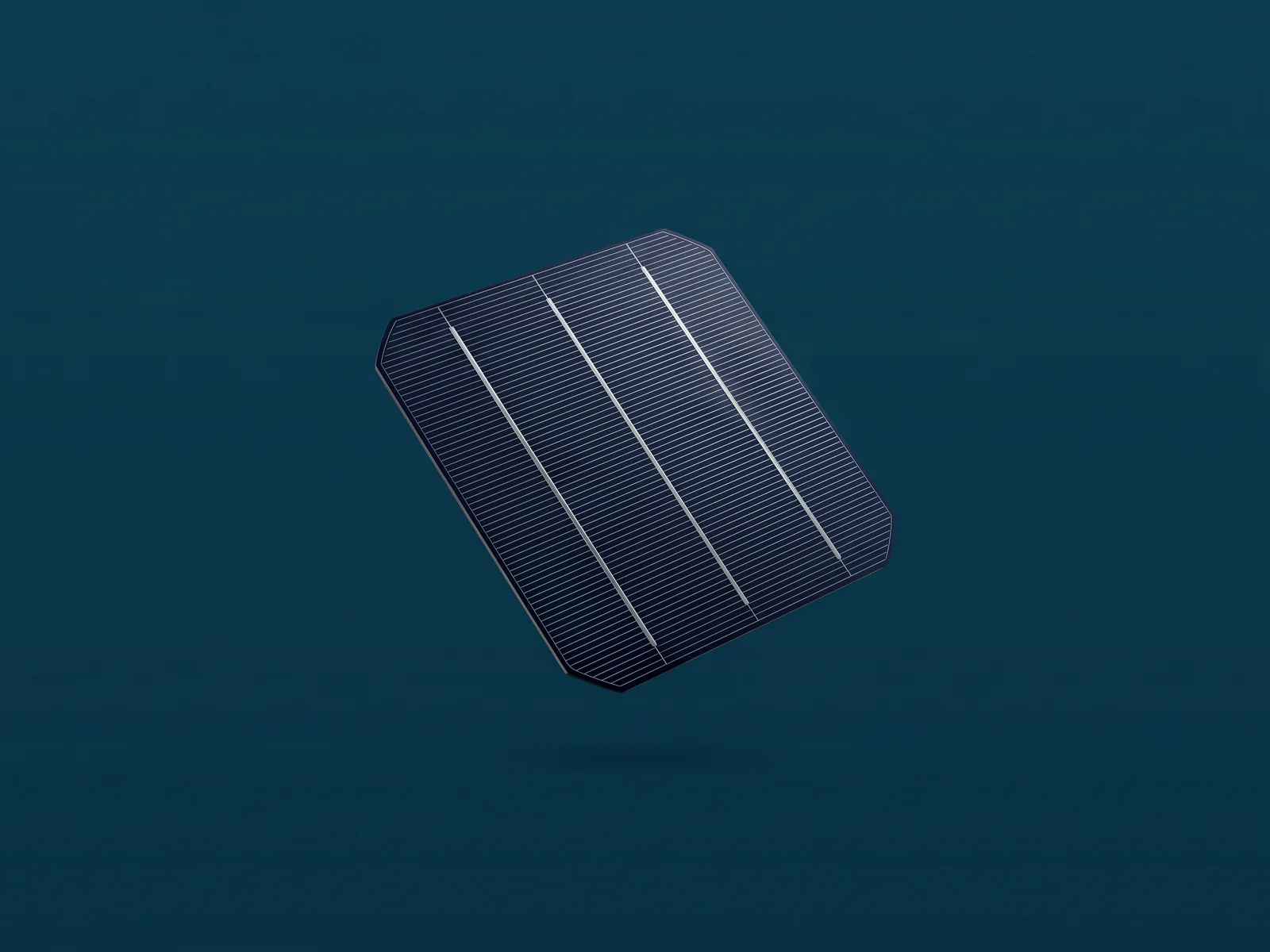
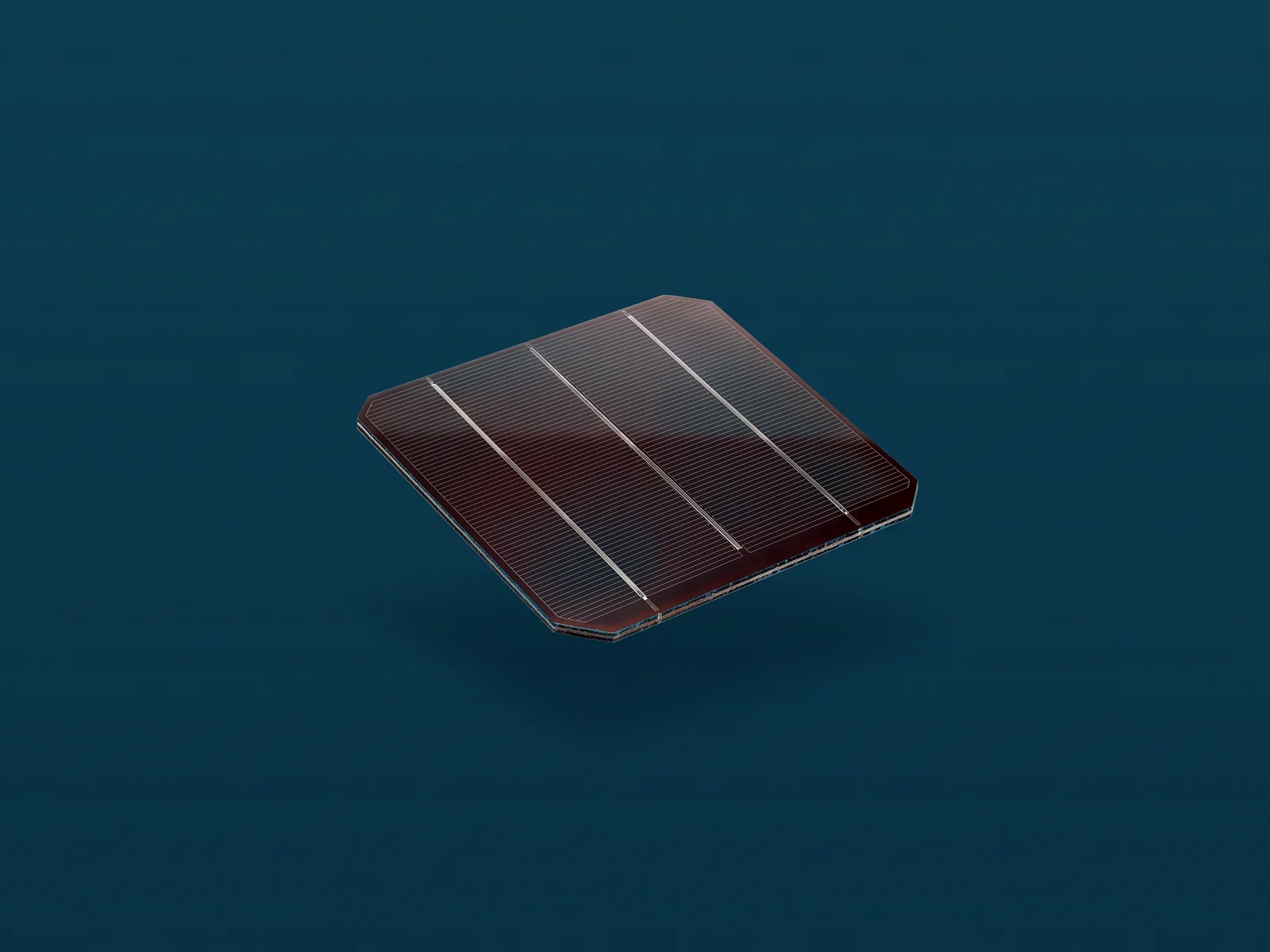
Thin-film scribing (P1–P3), perovskite and tandem cell interconnects, edge isolation and contact opening. Femtosecond pulses remove one layer at a time with minimal heat damage to the layer below, so dead area stays small and cells keep their efficiency.
Where femtosecond processing works in photovoltaics, from P1–P3 scribing of thin-film and perovskite modules to edge isolation, contact opening and tandem cells.
Thin-film scribing P1–P3
CIGS, CdTe and amorphous silicon modules are split into series-connected cells with three scribes: P1 through the first contact layer (molybdenum in CIGS, the transparent conductive oxide in CdTe and amorphous silicon), P2 through the absorber and P3 through the top contact. Femtosecond scribing keeps each line narrow and selective, so the dead zone between cells stays small.
Perovskite absorbers and their transport layers are thin and sensitive to heat. Femtosecond pulses scribe them with less of the decomposition and edge damage that longer pulses cause, which helps both the efficiency and the stability of the finished module.
Thin-film cells on metal foil or polymer substrates bend, so the scribe has to work on a flexible web without damaging the substrate. Ultrashort pulses keep the line selective even on thin polymer films.
Every scribe line costs area. Every heat zone costs efficiency.
Thin-film and perovskite modules are divided into narrow cells by laser scribing. The lines and the area between them produce no power, and heat from the scribe can damage the sensitive absorber next to it. Narrow, clean lines with minimal thermal damage turn directly into module output.
Heat damages the absorber
Nanosecond lasers scribe fast but leave melted edges, shunts and a heat-affected strip next to the line. In perovskite and other sensitive absorbers this damage lowers efficiency and long-term stability. Mechanical scribing leaves chips and debris.
What the process needs
Removal of one layer with minimal damage to the next
Narrow lines and a small dead zone between P1 and P3
Minimal shunting, melt or flaking at the line edge
High scribing speed on large panels
Remove one layer, keep the next
Femtosecond pulses ablate a single film cleanly and are gone before heat can reach the layer below. P1, P2 and P3 scribes stay narrow and well defined, even on heat-sensitive perovskite and organic absorbers.
Edge isolation and edge deletion
Before lamination, the layer stack is removed along the module border so the edge is electrically isolated and the encapsulant bonds to clean glass. Femtosecond removal leaves a clean glass surface with minimal cracking along the edge.
High-efficiency silicon cells are covered with passivation layers that have to be opened locally where the metal contacts go. The laser opens the dielectric in fine lines or dots with minimal damage to the silicon underneath, which would add recombination losses.
Perovskite-on-silicon and all-thin-film tandem cells stack two absorbers with very thin layers in between. Structuring one layer without touching the other needs pulses short enough that heat does not spread from the ablated film into the layers below.
They are the three laser lines that turn a continuous thin-film stack into series-connected cells. P1 separates the first contact layer, P2 opens the absorber so the second contact can reach the first, and P3 separates the second contact. The area between P1 and P3 produces no power.
Why femtosecond pulses for perovskite?
Perovskite absorbers decompose under heat. Femtosecond pulses remove material before heat can spread, so the line edges stay clean and the absorber next to the line is damaged far less.
Which layers can be processed?
Transparent conductive oxides, molybdenum and other back contacts, CIGS, CdTe, amorphous silicon, perovskite and organic absorbers, transport layers, and dielectric passivation layers on silicon.
Which wavelength is needed?
It depends on the layer. Infrared at 1030 nm suits many contact layers; green at 515 nm is absorbed more strongly by many absorbers. The best choice for each scribe is found by testing on the actual stack.
How fast is laser scribing?
Scribing speed depends on pulse energy, repetition rate and how the beam is split across heads. On large panels, throughput is set by the number of heads and the scan system as much as by the laser, and has to be measured on your stack and line design.
Which LITILIT laser fits photovoltaics?
Indylit 20 for thin-film, perovskite and tandem scribing, edge isolation and contact opening, with 1030 nm and optional 515 nm output. Indylit 10 for smaller-area structuring at 1030 nm.
How does buying a laser work?
Tell us your material, process and volume. An application engineer reviews your request and suggests a laser and configuration. You then receive a quotation with pricing, lead time, payment and support terms.
Tell us your material, process and volume. Our application engineers suggest a laser and configuration, and we send a quotation with pricing, lead time and support terms.